

Analysis of PCB Backdrill Technology
1. What is back drilling of PCB?
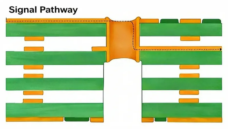
One of the challenges in PCB design and manufacturing is how to protect signal integrity issues. Back drilling, also known as controlled depth drilling, is used to remove conductive vias from copper cylinders in PCB vias. As part of vias, stubs can cause serious signal integrity in high-speed designs.

PCB back drilling
In addition, via stubs can cause signals to bounce back from the stub end, disrupting the original signal. In other words, if the stubs are long, the distortion will be severe.
To solve this problem, back drilling was performed, in whichmost of the via piles were removed by re-drilling with a slightly larger drill bit.

PCB back drilling
2.How PCB back drilling overcomes signal integrity issues
By using a slightly larger drill bit,these stubs are re-removed after plating through-hole fabrication. Drill the hole back to a predetermined and controlled depth that is close to, but not touching the last layer used by the hole.
Ideally, the remaining stub should be less than 10mils. The diameter of the back drill hole is larger than the diameter of the plated through hole. Typically, the diameter of the drilled bit is 8mils to 10mils larger than the diameter of the original drill bit. The reason is that the gap between the trace and the plane must be large enough to avoid accidentally drilling through the trace and plane adjacent to the back drill during the back drilling process.

Back drill before

After the back drill
3.Why do you need a back drill?
Back drilling can be used to shorten via stubs and can also interfere with high-speed signals, which typically result in short vias below 10 mils, weakening the copper pipe's ability to generate signal reflection.
For example: A through hole is drilled from the first layer to the tenth layer in a 10-layer stack. But your design requires signals from layer 1 to layer 3, and the vias will have a stub after layer 3. But the parts that are not used create high-frequency reflections and resonances.
Therefore, a back drill is required to remove excess copper plating after the third layer, and in addition, the back drill must be larger than the original size of the PTH, otherwise there is no way to remove all unwanted copper.
Here's the actual back drilling process:
1.In the image below, you can see the PCB with a via stub that extends beyond the signal path

PCB with via stubs
2.Use a slightly larger drill bit for back drilling

PCB back drilling with larger drill hole sizes
3.Reduce the via stub by back drilling
Reduce via stubs by back drilling
4.When to use a back drill?
It is generally recommended to consider adding back drilling when the circuit traces on the PCB board have signals at ≥1Gbps rate, but designing high-speed interconnect links is a complex systems engineering task that also requires consideration of factors such as the drive capability of the chip and the length of the interconnect link. Therefore, system interconnect link simulation is the most reliable way to determine whether back drilling is required.

PCB back drilling
General characteristics of PCB back drilling:
● The back is mostly hard board
● Generally used for more than 8 layers
● The thickness of the plate is greater than 2.5mm
● The minimum holding size is 0.3mm
● The back drill is 0.2mm larger than the via
● Back drill depth tolerance +/- 0.05MM
5.PCB back drilling process
● The locating hole is sealed with a dry film before plating.
● Plate holes with copper to create conductive paths.
● Create an outer layer of graphics on an electroplated PCB.
● After the outer graphic is made, the graphic plating is performed on the PCB. Before this process, it is important to dry film seal the locating holes.
● Back drilling is to use the positioning hole in the initial drilling process for alignment, and use the drill bit to back drill the electroplating hole that needs to be processed.
● After backdrilling, the plate needs to be cleaned to remove any residual cuttings that may be present in the backdrill.
● Inspect the board to verify that the back drilling process is performed accurately and that signal integrity is enhanced.

PCB back-drilling process
Example of a back drill:
Suppose there is a via from layer 1 and layer 12 in a 12-layer stack, but the via is only available from layer 1 to Signals for Layer 3.
So create a via stub after layers 3 and 12, which will create resonance and reflection at very high frequencies that will reduce the signal at the resonant frequency.
Therefore, a back drill is performed after layers 3 and 12 to remove the copper plating to reduce the length of the stub. The back drill should be larger than the original size, removing unwanted copper。

PCB back drill example
6.How much remaining stub length can be kept?
When backdrilling, you must calculate how much remaining stub length you can keep so that it doesn't affect PCB performance. The factor that determines this depends on several other factors, including: signal integrity and the actual manufacturing process
Generally reducing the maximum remaining stub length and increasing the via for back drilling increases manufacturing costs. The decision will depend on several interrelated factors, including the desired signal The table given below details the signal loss corresponding to the remaining stub length.

Signal loss corresponding to the remaining stub length
7.Difficulties in the back drilling process
1.Back drilling depth control
Back drilling is to use the depth control function of the drill bit to realize the processing of blind holes, and it's tolerance is mainly affected by the accuracy of the back drilling equipment and the tolerance of the thickness of the medium. In addition, its accuracy is easily affected by external influences, such as the resistance of the drill bit, the angle of the drill tip, the contact effect between the cover plate and the measuring unit, and the warping of the plate. Therefore, it is necessary to select appropriate drilling materials and drilling methods in production andcontrol their precision to achieve the best results.
2.Back drilling accuracy control
Back drilling is formed by secondary drilling according to the hole diameter of the primary drill, and the accuracy of the secondary drilling is very important. The expansion and contraction of the board, the accuracy of the equipment, the drilling method, etc. will affect the accuracy of the coincidence of the secondary drilling, which is very important for the quality control of the subsequent PCB process.
8.Advantages and disadvantages of PCB back drilling
1.Advantages
● Back drilling helps reduce signal degradation, ensuring a stronger and more reliable signal. Additionally, this technique helps minimize the impact of stubs on impedance matching, thereby reducing EMI/EMC emissions.
● Back drilling is also an effective way to prevent signal distortion issues. Vias stubs are known to cause deterministic jitter, which can be caused by signal crosstalk, EMI, and noise. By removing these stubs, back drilling can help eliminate sources of deterministic jitter, improve signal quality, and prevent signal distortion issues.
● Back-drilling helps minimize crosstalk between through-holes.
● By implementing back drilling, deterministic jitter in the signal can be reduced, thereby reducing the overall bit error rate of the signal
(BER) 。
● Reduce the excitation of resonant patterns.
● Minimize the use of buried and blind vias to streamline PCB production.
● Minimal impact on design and layout.
● Extended channel bandwidth;
● The cost will be lower compared to sequential lamination.
2.Disadvantages
One disadvantage of back drilling is that it is only suitable for high-frequency plates with a frequency range between 1GHz and 3GHz and no viable blind holes. In addition, special techniques must be used to prevent any injury to the traces and planes of the holes in the backplate.

 :
: :
: : A1 Building,Ditang Industrail B zone,Shajing Street,Bao'an
  :+86 13244860273

